The world of electronics is constantly evolving, with researchers striving to develop more efficient and reliable electronic components. One area of focus is the utilization of two-dimensional (2D) semiconducting materials, which possess unique optoelectronic properties that could revolutionize the field of electronics. Despite their potential advantages, integrating these materials with gate dielectrics has been a significant challenge, leading to the degradation of transistor performance. However, a recent breakthrough by a team of researchers from King Abdullah University of Science and Technology (KAUST), Soochow University, and other institutes worldwide offers new hope for the development of high-performance 2D transistors.
Optimally interfacing 2D semiconductors with gate dielectrics has proven to be a formidable task, as interfacial traps often arise, degrading the performance of transistors. However, the research team led by Yaqing Shen, Prof. Mario Lanza, and their colleagues introduced an innovative approach that could address this issue. By leveraging hexagonal boron nitride (h-BN) dielectrics and metal gate electrodes with a high cohesive energy, they were able to enhance the performance of transistors based on 2D semiconductors significantly.
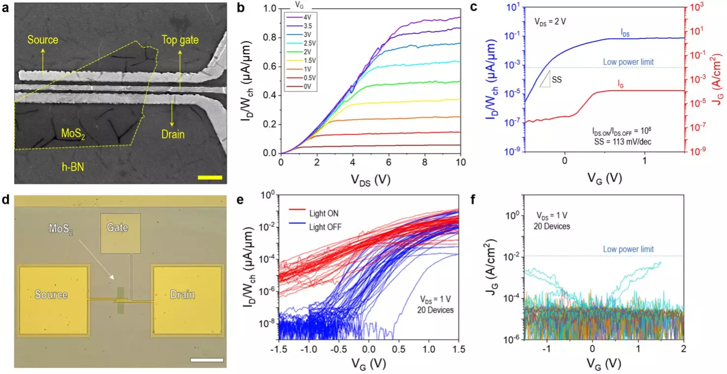
The team’s approach involved the utilization of chemical vapor deposited h-BN as dielectrics in fabricating over 1,000 devices. By using high cohesive energy metals such as platinum (Pt) and tungsten (W) in conjunction with h-BN gate dielectrics, they were able to achieve a 500-fold reduction in leakage current compared to transistors with gold (Au) electrodes. This breakthrough paved the way for the development of transistors with a vertical Pt/h-BN/MoS2 structure, demonstrating the potential of using CVD h-BN as an effective gate dielectric in 2D transistors.
One of the key findings of the research team was the discovery of a clean van der Waals interface between MoS2 and h-BN, which improved the reliability and performance of the transistors. Contrary to the belief that CVD h-BN is a poor gate dielectric, the team demonstrated that the proper selection of metal electrodes, such as Pt and W, enables its effective use in field-effect transistors with MoS2 channels. This advancement could open new possibilities for the development of highly reliable solid-state microelectronic circuits and devices based on 2D materials.
The groundbreaking research by Shen and her colleagues could potentially revolutionize the field of 2D semiconductor-based transistors, offering reduced leakage currents and increased dielectric strength. The use of high cohesive energy metals in conjunction with h-BN dielectrics has the potential to significantly enhance the performance of 2D transistors and pave the way for the development of ultra-small, fully 2D transistors. Furthermore, this research opens the door for other research groups to explore similar approaches and materials, potentially leading to further advancements in 2D semiconductor-based devices.
The development of 2D semiconductor-based transistors holds great promise for the future of electronics. The innovative approach introduced by the research team from KAUST, Soochow University, and other institutes worldwide demonstrates the potential of using h-BN dielectrics and high cohesive energy metal electrodes to improve the performance and reliability of 2D transistors. With further research and exploration, the realm of 2D electronics may soon witness significant advancements, paving the way for the realization of highly efficient and reliable electronic components.


Leave a Reply