The realm of semiconductor research has long fascinated scientists and engineers alike, weaving together complex theories and practical applications that underpin much of today’s electronic technology. Recent notable advancements have emerged from UC Santa Barbara (UCSB), where a team led by Bolin Liao has made a groundbreaking discovery: for the first time, researchers have succeeded in capturing a dynamic “movie” of electric charges as they traverse the interface between two dissimilar semiconductor materials. This accomplishment not only advances our understanding of semiconductor behaviors but also holds significant implications for future electronic devices, renewable energy technologies, and beyond.
Understanding how electric charges, known as photocarriers, behave within semiconductor materials is paramount, especially in the context of solar cells and other devices reliant on light absorption. The process is fundamentally about the movement of electrons, energized when sunlight interacts with semiconductor compounds. When these energized electrons separate from their positively charged counterparts, or “holes,” they generate an electric current, which can subsequently be harvested for energy. However, this valiantly sought-after energy is typically lost in the first few picoseconds after excitation, rendering most conventional systems inefficient.
Researchers have long speculated about the behavior of these so-called “hot” carriers—their high-energy state momentarily yielding unprecedented potential for energy applications. Nevertheless, because hot carriers typically dissipate their energy incredibly quickly, this essential phase of semiconductor operation remained largely obscured within indirect measurements and theoretical discussions. The research by Liao and his team fills a critical gap in semiconductor research by offering direct visualization of how these carriers maneuver across material boundaries.
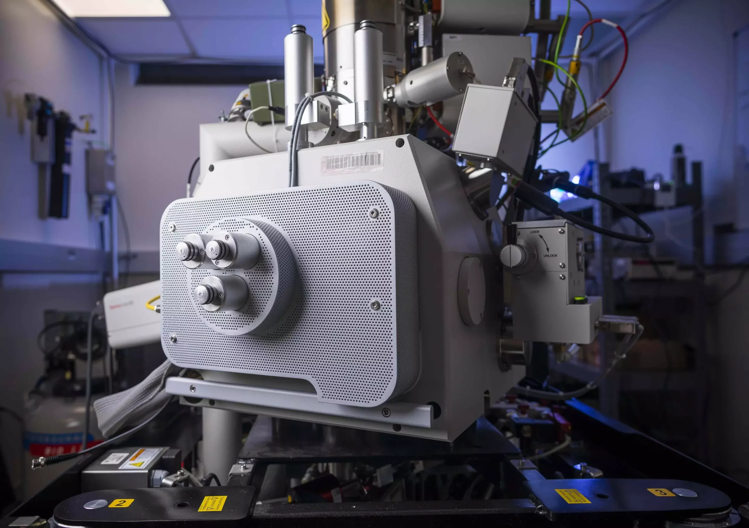
The research hinged on the innovative use of scanning ultrafast electron microscopy (SUEM), an advanced technological technique that enables scientists to scrutinize the behavior of electrons with unparalleled time and spatial resolution. By incorporating ultrafast laser pulses as a picosecond-scale shutter, researchers could synchronize the electron beam to capture the fleeting moment when photocarriers transition across the interface of silicon and germanium—a pairing known for its vast applications in photovoltaics and telecommunications.
This pioneering imaging technique proved revolutionary, allowing Liao’s team to map electronic movements with unprecedented clarity. By observing how charges behave when excited in various regions—specifically examining the effects of a junction potential—the team collected valuable real-time data. Their findings revealed that while photocarriers display high mobility when excited in uniform material regions, their speed diminishes upon nearing the heterojunction. This crucial insight into trapping conditions at the interface depicts a critical interaction—a challenge semiconductor device designers must navigate when creating efficient energy conversion systems.
The implications of this research extend far beyond academic curiosity. By establishing a direct observational link between theory and practice, semiconductor scientists can now refine their knowledge of charge carrier dynamics. Notably, addressing the challenges posed by charge trapping within heterojunctions can lead to improved energy efficiency in devices, particularly in photovoltaic systems. The ability to contemporaneously assess these interactions offers an empirical foundation for improving semiconductor designs and optimizing device performance, thereby contributing toward a more sustainable future.
Moreover, the study resonates with the legacy of the late UCSB professor Herb Kroemer, who fundamentally altered the semiconductor landscape by introducing the concept of heterostructures in the late 1950s. By asserting that “the interface is the device,” Kroemer’s insights paved the way for modern-day microelectronics, and Liao’s visualization work reinforces this ongoing tradition of innovation at UCSB.
The collaboration between Liao’s team and researchers at UCLA exemplifies the interdisciplinary nature of scientific breakthroughs. By blending principles of mechanical engineering, materials science, and electrical engineering, they have provided the academic and industrial communities with newfound capabilities to investigate semiconductor materials. The first “movie” of charge movement across a heterojunction not only enhances our comprehension of photocarrier behavior but also solidifies a template for future studies.
The insights gleaned from this research invite further exploration, suggesting potential avenues for developing next-generation semiconductor devices that can harness energy more effectively. As researchers continue to decode the intricate behaviors of hot carriers, they take monumental steps toward bridging the gap between theory and application, shaping a promising trajectory for electronic innovation in the years to come.


Leave a Reply