
Recent advancements in material science herald promising developments, particularly in the field of antiferroelectric materials. Unique in their electrical characteristics, these materials present groundbreaking applications in energy storage, sensors, and memory devices. Understanding their electronic properties is vital for the evolution of state-of-the-art technologies, yet researchers have traditionally grappled with the challenge of imaging such materials effectively. A trailblazing study by scientists at the University of Chicago sheds light on these intricacies and opens a plethora of new avenues for exploration and application.
Resolving the Imaging Conundrum
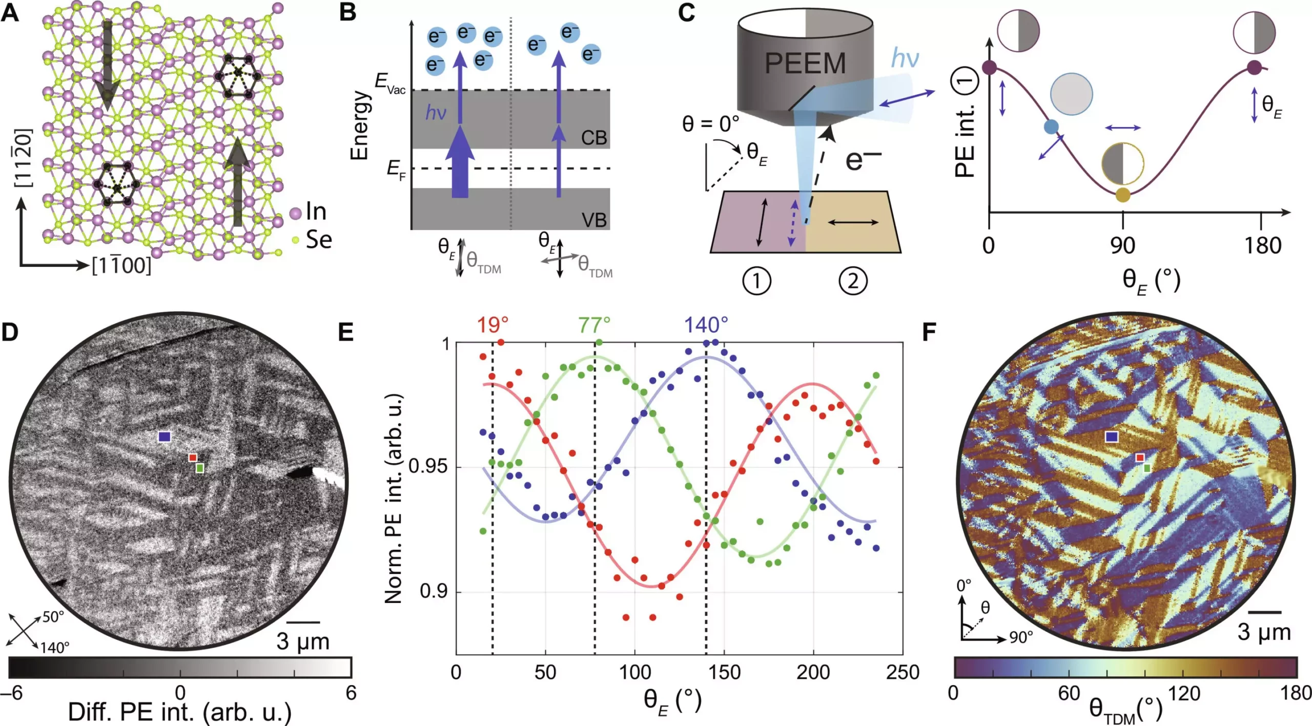
The difficulty in visualizing the electronic properties of antiferroelectric materials has long stymied researchers eager to uncover their true capabilities. Conventional imaging methods often fall short, lacking the spatial resolution and contrast necessary to differentiate between the various domains within these complex materials. Sarah King, an Assistant Professor of Chemistry and the lead author of the study published in *Science Advances*, highlights a critical gap: “One of the major hurdles is that we don’t have a great way of determining whether something is antiferroelectric because we lack the means to visualize the domains.”
By employing an innovative approach that enhances traditional imaging techniques, King’s team has made a substantial leap in this area. The breakthrough employs a method known as polarization-dependent photoemission electron microscopy, providing enhanced visual capabilities to investigate antiferroelectric materials on a nanoscale. This technique paves the way not only for better imaging but also for a deeper comprehension of the materials’ electronic structures.
A Deep Dive into Antiferroelectricity
Antiferroelectric materials boast a rare arrangement of electric dipoles that cancel each other out, leading to a net neutrality in polarization. This intrinsic property forms the basis for their dynamic use in electronics. When subjected to an external electric field, these materials can transition to a higher energy state, allowing electric dipoles to align more freely, further enhancing their potential in applications such as energy storage and advanced sensor technology.
The idea of harnessing this unique property could be transformative. Consider how much more efficient energy storage solutions would be if they incorporated materials that can shift states quickly and reliably. In light of rising global energy demands, tapping into antiferroelectricity for improved storage systems could yield exceptional benefits.
The Role of Innovative Imaging Techniques
King’s team’s pioneering imaging method represents a step toward unraveling the complex behavior of these materials, revealing the arrangement and orientation of antiferroelectric domains with unprecedented clarity. This provides researchers with a detailed map, allowing them to explore phenomena such as the dynamics of domain switching and phase transitions. Such granular insight into the structure of materials can lead to further innovations in material customization—an essential step for the effective implementation of antiferroelectric-based technologies.
Through this advance, King emphasizes a broader vision: “I believe that having new imaging techniques with such high spatial resolution is incredibly powerful. It’s going to play a critical role in the development of new materials.” The implications of this technology ripple across various fields, from semiconductor manufacturing to energy-efficient computing, suggesting that we stand on the brink of a significant industrial transformation.
Collaborative Efforts and Future Prospects
The importance of collaboration in scientific research cannot be overstated, as showcased by the diverse team involved in this groundbreaking study at the University of Chicago. With contributions from graduate students, postdoctoral researchers, and even partnerships with institutions like Oak Ridge National Laboratory, this research embodies the collaborative spirit necessary for innovation. It signals a future where cross-disciplinary efforts can yield extraordinary results that propel material science into uncharted territories.
As researchers delve deeper into the electronic properties of antiferroelectric materials, the potential for novel applications becomes ever more tantalizing. Enhanced imaging techniques offer the lens through which we can better understand not only how these materials behave but also how to manipulate their properties for practical solutions to real-world problems. The promise of antiferroelectric materials in a technologically advancing society could well redefine our approach to energy usage and storage, making this an exciting time for scientists and engineers alike.
Leave a Reply