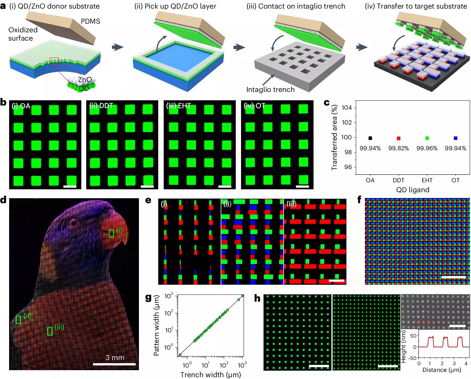
In a groundbreaking development, a research team has introduced a double-layer dry transfer printing technology that has the potential to revolutionize the world of augmented reality (AR) and virtual reality (VR). The research, recently published in Nature Photonics, showcases the advancements made in light-emitting and electron-transferring layers simultaneously transferred onto a substrate. This innovation is pivotal in enhancing the immersive experience for users engaged in AR, VR, and wearable display technologies.
The demand for AR, VR, and wearable displays has been steadily rising due to recent advancements in wearable, mobile, and Internet of Things (IoT) technologies. With wearable displays becoming more commonplace on wrists and eyes, the need for conveying large amounts of information on small screens with ultrahigh-definition patterning is essential to prevent dizziness among users. Quantum dot nanoparticles have emerged as the future of display light-emitting materials due to their high color purity and reproduction capabilities.
While conventional dry transfer printing techniques have shown potential in achieving ultrahigh-definition pixels, they have been hindered by low luminescence efficiency of under 5%. To address this limitation, DGIST Professor Ji-woong Yang, along with UNIST Professor Moon-kee Choi and Taeg-hwan Hyun from the IBS Nanoparticle Research Center, collaborated to develop a new double-layer dry transfer printing technology. This innovative approach allows for the production of bright light even at low currents, enabling high-resolution pixel patterning and the creation of light-emitting devices with ultra-high definition and efficiency.
The research team’s efforts have resulted in the development of high-density double-layer thin films with an external quantum efficiency (EQE) of up to 23.3%. By reducing interfacial resistance, electron injection is facilitated, and leakage charge transport is controlled during the fabrication process of light-emitting devices. This achievement aligns closely with the maximum theoretical efficiency of quantum dot light-emitting devices. Additionally, the team successfully demonstrated the creation of ultrahigh-definition patterns of quantum dots up to 25,526 PPI, with an 8 cm x 8 cm area achieved through repeated printing, indicating the feasibility of mass production for commercialization purposes.
Professor Ji-woong Yang expressed his satisfaction with the results, highlighting the significance of the new technology in producing light-emitting devices that are both ultrahigh-definition and high efficiency. The potential implications of this technology for higher resolution screens in VR and AR are immense, as stated by Professor Moon-kee Choi. The collaborative efforts of the research team have paved the way for a new era of enhanced AR, VR, and wearable displays, promising a more immersive and captivating experience for users worldwide.


Leave a Reply