Antiferromagnets represent a fascinating area of materials science, distinguished by the unique arrangement of magnetic moments among their atomic structure. Unlike ferromagnets, where magnetic moments align in parallel, antiferromagnets display a staggered orientation; adjacent magnetic moments oppose each other. This intrinsic property leads to no overall magnetization, a feature that, while seemingly limiting, holds remarkable promise for future technological advancements, particularly in spintronics and electronics.
At the forefront of this research is a recent breakthrough by scientists at Harvard University who have identified an antiferromagnetic diode effect in a specific material known as MnBi2Te4. This finding is significant as it could unlock new pathways for the design and implementation of novel electronic devices capable of operating with enhanced efficiency and functionality.
The antiferromagnetic diode effect is characterized by the ability to permit electrical currents to flow predominantly in one direction within a device, akin to traditional diodes. However, the distinction here lies within the properties of the material, particularly its centrosymmetric crystal structure that complicates the theoretical understanding of charge separation. This discovery challenges existing paradigms of conductivity and charge movement, thereby opening a dialogue for re-evaluating how we approach the engineering of electronic components.
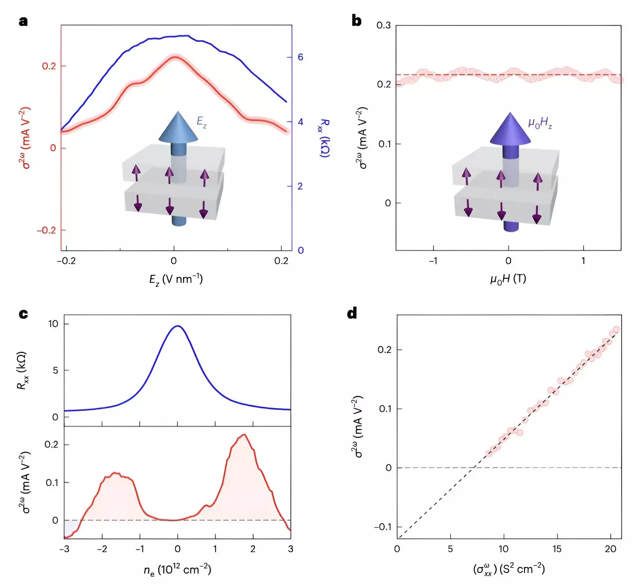
The research conducted by the Harvard team, as detailed in their recent publication in *Nature Electronics*, demonstrates that the even-layered MnBi2Te4 can behave as a diode without the typical directional charge separation expected in conventional materials. This finding not only extends the realm of possible applications but also invites further research into the implications of this effect in existing and future technologies.
In their comprehensive study, the research team developed devices using two distinct configurations of electrodes: Hall bar electrodes and radially distributed electrodes. Employing these varied setups enabled them to explore new dimensions of the antiferromagnetic diode effect. Through rigorous experimental methods, including spatially resolved optical techniques and electrical sum frequency generation (SFG) measurements, they provided compelling evidence of nonlinear transport behavior in the material under investigation. Such rigorous experimental design is crucial for reliable findings, facilitating the possibility of practical applications.
By examining the unique electronic characteristics of even-layered MnBi2Te4, the researchers could observe significant second-harmonic transport properties. These behaviors raise exciting prospects for applications in fields such as in-plane field-effect transistors and energy harvesting technologies, where efficiency and effectiveness are paramount.
The potential implications of the antiferromagnetic diode effect extend beyond mere theoretical interest. The possibility of leveraging this property to develop antiferromagnetic logic circuits puts a spotlight on an impending evolution in computational technology. These circuits promise to be faster, more energy-efficient, and capable of performing complex operations that current technologies struggle with due to inherent limitations. Furthermore, the integration of microwave energy harvesting devices rooted in this effect illustrates a tangible path towards more sustainable technological solutions.
The authors of the study succinctly highlight that the antiferromagnetic diode effect could redefine non-linear applications and integrate seamlessly into existing frameworks of electrical engineering. This paradigm shift could inspire a new era of innovation where quantum materials and spintronic devices play a pivotal role in shaping the future of electronics.
The exploration of the antiferromagnetic diode effect within even-layered MnBi2Te4 reveals significant findings that can reshape our understanding of material properties and their applications in technology. As researchers delve deeper, the connection between fundamental physics and practical engineering becomes increasingly evident, promising to pave the way for advanced devices that could enhance performance across numerous domains. The Harvard team’s work stands as a valuable contribution to the field, encouraging further investigation into the potential of antiferromagnetic materials in developing next-generation technologies. The convergence of quantum mechanics and electronic engineering continues to offer an intriguing landscape ripe for discovery and innovation.


Leave a Reply