Organic semiconductors have come a long way since their first appearance in the 1980s. With applications ranging from OLED displays to biosensors, these materials have found a significant place in the world of technology.
One of the main challenges faced in the development of organic semiconductor devices is achieving ultra-high resolutions. While inorganic semiconductors like silicon have reached dimensions as small as 1 nm using photolithography, organic materials present a different set of challenges due to their sensitivity to UV light and solvents.
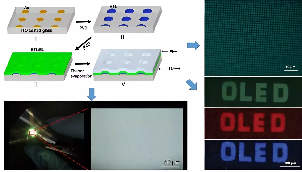
In a recent review published in the journal Wearable Electronics, scientists detailed their work in developing a new technology for fabricating ultra-high-resolution organic semiconductor devices. The key to their success lies in the approach of “first surface patterning and then patterned growth.”
By patterning the substrate surface before introducing organic materials, the researchers were able to avoid damaging the functionalities of the materials. This method allowed for the selective growth of organic semiconductor molecules at designated areas, resulting in the formation of high-resolution devices on substrates.
The implications of this breakthrough are vast, especially in the realm of wearable electronics. The ability to achieve resolutions of over 20K ppi opens up new possibilities for next-generation displays. With the demand for multifunctional systems on a chip increasing, the integration of high-resolution organic semiconductor devices will play a crucial role in the development of future wearable technologies.


Leave a Reply